Discovery of a New Photonic Crystal where Light Propagates through the Surface without being Scattered
Achievable Even by Silicone Alone; Developments of New Functions through Integration with Semiconductor Electronics
2015.06.08
(2015.09.18 Update)
National Institute for Materials Science (NIMS)
NIMS MANA researchers elucidated a new principle whereby electromagnetic waves including light propagate on the surface of a photonic crystal without being scattered.
Abstract
- Xiao Hu, Principal Investigator of the International Center for Materials Nanoarchitectonics (MANA), National Institute for Materials Science (NIMS), and Long-Hua Wu, NIMS Junior Researcher, elucidated a new principle whereby electromagnetic waves including light propagate on the surface in a photonic crystal without being scattered. By merely slightly adjusting positions of insulator or semiconductor cylinders (nanorods) in a honeycomb lattice, electromagnetic waves can propagate without being scattered even at corners of crystal or by defects. Since this property can be achieved even by a semiconductor, such as silicone, alone, developments of new functions are expected via integrating information processing functions achieved by the well-established semiconductor electronics and the excellent propagation property of electromagnetic waves.
- In recent years, active studies have been conducted on materials with topological properties where unique properties appear on surfaces of materials. Suppressions of scattering of light by defects in conventional photonic crystals is also expected in topological photonic states. However, special materials were required to create topological photonic crystals.
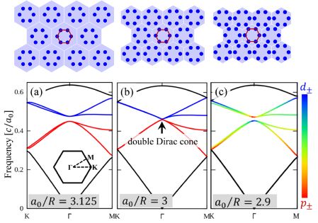
- These researchers discovered a new principle to realize a topological photonic crystal by merely adjusting positions of insulator or semiconductor nanorods in a honeycomb lattice, without using any complicated material or structure. When hexagonal clusters are formed by adjusting positions of clinders, electromagnetic modes carrying on spin, a feature conventionally specific to electrons, appear. As a result, it was theoretically clarified that a photonic crystal exhibits topological properties when the separation between hexagonal clusters is narrowed from that of the honeycomb lattice.
- Since the nanorods can be formed by silicone, developments of new functions and devices are expected through integration with existing silicon-based electronics.
- This research was partially supported by “Topological Quantum Phenomena in Condensed Matter with Broken Symmetries,” Grant-in-Aid for Scientific Research on Innovative Areas, Ministry of Education, Culture, Sports, Science and Technology. The research results were published in Physical Review Letters, a journal of the American Physical Society, online on June 3, 2015 (local time).

Above: Schematic of photonic crystals consisting of cylinders in a honeycomb lattice viewed from above. Photonic crystals obtained by dividing the nearest neighboring cylinders into hexagonal clusters, and widening (left) or narrowing (right) the separation between hexagonal clusters from the original honeycomb lattice (middle), while keeping the shape and size of hexagons. Below: Relationship between the wave number and frequency of the photonic crystal in each case. Here, a0 denotes the distance between the hexagonal clusters as measured from their center, and R denotes the length of one side of the hexagon.
