nano tech 2013
International Nanotechnology Exhibition & Conference
Schedules 2013.01.30 - 02.01 Finished
NIMS to particiapate in "nano tech 2013", the world's largest international exhibition of nanotechnology.
What's "nano tech" ?

With the evolution of nanotechnology, application fields have broadened. Recently, nanotechnology based products and technologies became a key factor for the solution of important issues such as IT & electronics field, medical & health care, biotechnology, environment & energy problems.
NIMS exhibits the research poster and hold the lecture in the booth every year.
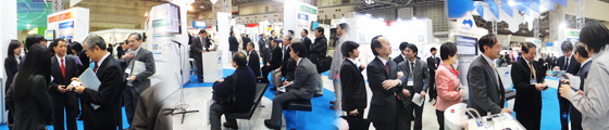
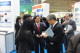
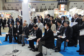
Images from "nano tech 2012"
NIMS Exhibition (Tentative)
Research Poster
| Category | Title | Name |
|---|---|---|
| Materials for Opto-electronics | Soft and Tunable Colloidal Crystal Lasers | Seiichi Furumi |
| Ultracompact photonic circuit devices using exciton polaritons in organic nanofibers | Ken Takazawa | |
| Paintable, Nonvolatile, Luminescent Liquids | Hiroshi Nakanishi | |
| Nanoscale Investigation and Fablication | Nano-characterization and Nano-fabrication by Scanning Helium Ion Microscopy(SHIM) | Keiko Ohnishi |
| Matrerials for Nanodevices | Diamond-based Field Effect Transistors for Next-Generation Power Electronic Devices | Masataka Imura |
| Nano-ionics device achieved by local ion migration | Kazuya Terabe | |
| Organic molecules for single-electron memory device | Yutaka Wakayama | |
| Materials for Bio and Life Saving | Smart nanomaterials for the enrichment of biomarkers | Mitsuhiro Ebara |
| Magnetic Particle Imaging and Hyperthermia Treatment of Cancer using Magnetic Nanoparticles | Hiroaki Mamiya | |
| Materials for New Energy | Graphene Supercapacitors of High Energy Density | Tang Jie |
| New Solar Cell Materials using Si Nanostructures | Naoki Fukata | |
| Catalytic metal/organic nano-hybrids for fuel-cell electrodes | Hideki Abe | |
| Control of atomic & grain structure to realize highly effective thermoelectric materials | Takao Mori | |
| Theoretical Studies in Nanomaterials | Discovery of new mechanism of nucleation | Masamichi Nishino |
| Engineering quantum effects in topological insulators:theoretical study | Akihiro Tanaka | |
| The Elements Strategy Intiative Center for Magnetic Materials (ESICMM) | Tetsu Hirosawa | |
| Advanced Measurements using Brilliant and Monochromatic Synchrotron X-rays at NIMS Beamline at SPring-8 | Osami Sakata | |
| NIMS Nanotechnology Platform : Advanced User Facilities Network with High-Level Technical Service | Keijiro Hirahara | |
| Low-Carbon Research Network Japan | Katsumi Suzuki | |
| GREEN providing Open-lab and Short RA system | Kotobu Nagai | |
| TIA Nano-Green: Membership-based Open Innovation | Kazuo Nakamura |
Lectures
Wednesday, Jan 30 2013
| Time | Title/Theme | Speaker |
|---|---|---|
| 10:30-10:45 | Nano-characterization and Nano-fabrication by Scanning Helium Ion Microscopy(SHIM) | Keiko Ohnishi |
| 11:00-11:15 | Discovery of new mechanism of nucleation | Masamichi Nishino |
| 13:30-13:45 | Graphene Supercapacitors of High Energy Density | Tang Jie |
| 14:00-14:15 | TIA Nano-Green: Membership-based Open Innovation | Kazuo Nakamura |
| 14:30-14:45 | Control of atomic & grain structure to realize highly effective thermoelectric materials | Takao Mori |
| 15:00-15:15 | Ultracompact photonic circuit devices using exciton polaritons in organic nanofibers | Ken Takazawa |
| 15:30-15:45 | The Elements Strategy Intiative Center for Magnetic Materials (ESICMM) | Tetsu Hirosawa |
Thursday, Jan 31 2013
| Time | Title/Theme | Speaker |
|---|---|---|
| 10:30-10:45 | Engineering quantum effects in topological insulators:theoretical study | Akihiro Tanaka |
| 11:00-11:15 | Magnetic Particle Imaging and Hyperthermia Treatment of Cancer using Magnetic Nanoparticles | Hiroaki Mamiya |
| 13:30-13:45 | Diamond-based Field Effect Transistors for Next-Generation Power Electronic Devices | Masataka Imura |
| 14:00-14:15 | Paintable, Nonvolatile, Luminescent Liquids | Hiroshi Nakanishi |
| 14:30-14:45 | Organic molecules for single-electron memory device | Yutaka Wakayama |
| 15:00-15:15 | Low-Carbon Research Network Japan | Yasuo Koide |
| 15:30-15:45 | NIMS Nanotechnology Platform : Advanced User Facilities Network with High-Level Technical Service | Daisuke Fujida |
Friday, Feb 1 2013
| Time | Title/Theme | Speaker |
|---|---|---|
| 10:30-10:45 | Advanced Measurements using Brilliant and Monochromatic Synchrotron X-rays at NIMS Beamline at SPring-8 | Osami Sakata |
| 11:00-11:15 | New Solar Cell Materials using Si Nanostructures | Naoki Fukata |
| 13:30-13:45 | Nano-ionics device achieved by local ion migration | Kazuya Terabe |
| 14:00-14:15 | Soft and Tunable Colloidal Crystal Lasers | Seiichi Furumi |
| 14:30-14:45 | Smart nanomaterials for the enrichment of biomarkers | Mitsuhiro Ebara |
| 15:00-15:15 | Catalytic metal/organic nano-hybrids for fuel-cell electrodes | Hideki Abe |
Pictures from Previous Year (nano tech 2012)


Related File / Link
Summary
- Event Title
-
nano tech 2013
International Nanotechnology Exhibition & Conference - Venue
- East Exhibition Hall 4, 5, 6 & Conference Tower, Tokyo Big Sight, Japan
3-21-1 Ariake, Koto-ku, Tokyo 135-0063, JAPAN
- Schedules Hours
-
2013.01.30 - 02.01
10:00-17:00 - Registration Fee
- 3,000 Japanese Yen (Free admission with online registration)
- Organized by
- nano tech executive committee
- For detail
- Please see the "nano tech 2013" website.
- Supported by (*tentative)
- Cabinet Office Government of Japan /Ministry of Internal Affairs and Communications /Ministry of Education, Culture, Sports, Science & Technology /Ministry of Agriculture, Forestry and Fisheries /Ministry of Economy, Trade & Industry /Embassy of the United States of America /Embassy of the Islamic Republic of Iran in Tokyo /British Embassy Trade & Investment Department /Embassy of the Kingdom of the Netherlands /Embassy of Canada /Embassy of Switzerland /Embassy of Spain - Economic and Commercial Office /Embassy of the Republic of Korea /Royal Thai Embassy /Embassy of the Czech Republic /Embassy of the Federal Republic of Germany /Finnish Funding Agency for Technology and Innovation (Tekes) /French Trade Commission - Ubifrance, Embassy of France in Japan /Embassy of the Kingdom of Belgium /Embassy of the Russian Federation in Japan /National Institute of Information and Communications Technology (NICT) /National Institute for Materials Science (NIMS) /RIKEN /Japan Science and Technology Agency (JST) /National Institute of Advanced Industrial Science and Technology (AIST) /New Energy and Industrial Technology Development Organization (NEDO) /Japan External Trade Organization (JETRO) /National Institute for Environmental Studies (NIES) /Keidanren (Japan Business Federation) /Nanotechnology Business Creation Initiative (NBCI)
- In cooperation with (*tentative)
- The Japan Society of Applied Physics (JSAP) / The Society of Polymer Science, Japan/ The Chemical Society of Japan (CSJ)
Inquiry about this page
- Secretariat of nano tech executive committee
-
ICS Convention Design, Inc.
Chiyoda Bldg.1-5-18, Sarugakucho, Chiyoda-ku,Tokyo 101-8449, JAPAN
Phone:+81-3-3219-3567
Fax:+81-3-3219-3628
E-Mail: nanotech=ics-inc.co.jp(Please change "=" to "@")
| Sun | Mon | Tue | Wed | Thu | Fri | Sat |
|---|---|---|---|---|---|---|
|
1
|
2
|
3
|
4
|
|||
|
5
|
6
|
7
|
8
|
9
|
10
|
11
|
|
12
|
13
|
14
|
15
|
16
|
17
|
18
|
|
19
|
20
|
21
|
22
|
23
|
24
|
25
|
|
26
|
27
|
28
|
29
|
30
|
31
|