The article of Atomic Switch, developed by Nanomaterials Laboratory, was featured in January’s nature top ten
2005.01.06
(Jan. 6, 2005) Nanomaterials Laboratory (NML) in cooperation with RIKEN and JST successfully developed an ultimate nano-device called Atomic Switch by controlling atomic transfer on the nanoscale.
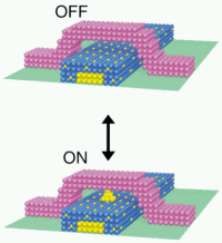
Figure: Structure of the Atomic Switch and the operation principle.
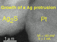
Movie: Metallic cluster formation used in operation of the Atomic Switch (25 seconds). Much smaller cluster is formed in actual operation of the Atomic Switch.
NML also fabricated basic memory and logic circuits by using the Atomic Switch and verified their excellent operating properties. The article titled “Quantized conductance atomic switch” was published in the 6 January 2005 issue of nature and was featured in that month's nature top ten: one of the ten articles most frequently downloaded from the nature website.
Summary:
The formation and annihilation of a metallic cluster is controlled in a gap of about 1 nm between a solid electrolyte electrode (lower) and a metallic electrode (upper). By applying a negative bias voltage to the metallic electrode, metallic ions in the solid electrolyte electrode are reduced and deposited at the surface of the solid electrolyte electrode, resulting in the formation of a metallic cluster between two electrodes to turn on the switch (bottom). Then, by applying a positive bias voltage, the deposited metallic atom dissolves into the solid electrolyte electrode and the metallic cluster is annihilated; the switch is turned off (top).
Movie(File size: 9MB / AVI) (AVI:9.08MB) Metallic cluster formation used in operation of the Atomic Switch (25 seconds). Much smaller cluster is formed in actual operation of the Atomic Switch.
The formation and annihilation of a metallic cluster is controlled in a gap of about 1 nm between a solid electrolyte electrode (lower) and a metallic electrode (upper). By applying a negative bias voltage to the metallic electrode, metallic ions in the solid electrolyte electrode are reduced and deposited at the surface of the solid electrolyte electrode, resulting in the formation of a metallic cluster between two electrodes to turn on the switch (bottom). Then, by applying a positive bias voltage, the deposited metallic atom dissolves into the solid electrolyte electrode and the metallic cluster is annihilated; the switch is turned off (top).